


NASA’s Engineering and Safety Center (NESC) investigated two cracked thick-film chip resistors found during environmental testing of printed circuit board assemblies. The alumina substrates cracked during thermal cycling after vibration testing, causing intermittent open circuits at hot temperatures. Although the resistor lot met procurement requirements and investigators found no evidence of manufacturing defects or vibration fatigue, the analysis identified board bending, component orientation, excessive solder and mounting stress as factors that may increase the risk of cracking in large ceramic components.
Background
Chip resistors are widely used in NASA projects, but cracking of their alumina substrates during vibration or thermal cycling has not previously been reported to NESC. In this case, two cracks were found in thick-film chip resistors during post-vibration thermal cycling.
Both failures produced intermittent open circuits during hot dwells, with the circuits recovering at room temperature. The cracks appeared at the midpoint of each resistor and ran parallel to the termination. The two resistors were installed in similar locations near the edges of two identical boards. In both cases, the crack ran across the resistor’s short axis, perpendicular to its long axis, consistent with bending of the component. The failed resistors showed no signs of pre-existing defects.
Investigation and failure analysis
The initial theory was that vibration had damaged a potentially defective resistor because both failed components came from the same manufacturing lot. However, the lot met the requirements of procurement specification MIL-PRF-55342. Additional testing found no direct evidence that the lot was defective, and there was no evidence of an increased risk of resistor defects within production lots.
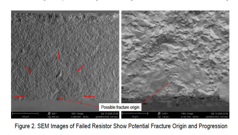
An independent failure analysis concluded that the cracks resulted from bending and tensile forces. No visible defect identified a clear crack-initiation site. Each resistor exhibited a single, straight crack across its short axis, indicating a non-torsional bending or tensile failure.
The damage pattern was not consistent with cyclic fatigue, making fatigue failure during vibration less likely. Optical microscopy and scanning electron microscopy (SEM), conducted independently of NESC, also found no clear defect location showing the initiation and progression of fatigue damage in either resistor. As a result, a defective resistor lot or vibration-induced fatigue was considered less likely to be the root cause.
Potential contributing factors
No direct root cause was identified. However, the investigation highlighted several factors that may require additional design consideration when large-footprint ceramic components are placed near the edges of printed circuit boards. Manufacturing or installation can cause boards to warp or twist, creating stress that may crack ceramic components.
- The relatively large resistor, case size 2512, was installed near the board edge with its long axis parallel to the edge, making it more vulnerable to board bending.
- Excess solder extended onto the top pad of the resistor termination.
- Board bending or twisting could have created excessive bending moments or loads.
- Rigidly mounting the board to a frame could have increased and amplified bow or torsional stresses.
- Non-optimal fastener-tightening patterns could have concentrated installation stresses near the resistor.
Assembly guidelines for ceramic components
Based on this experience, the following practices should be considered when assembling ceramic-body components onto printed circuit boards.
Component orientation
To reduce the effects of global and local board bending, avoid orienting the long axis of large-footprint ceramic components parallel to the edge of a nearby printed circuit board.
Finite element analysis
If large components must be placed near a board edge, perform a thorough finite element analysis to demonstrate that the component has adequate stress and displacement margins.
Solder fillet height
Avoid allowing solder to contact the top surface of the component terminal. Solder on the top of the terminal can create a rigid joint that transfers board deflection directly to the ceramic, increasing the risk of cracking. Component manufacturers should be consulted because they may specify limits for solder fillet height.
Solder-joint inspection
Inspect the physical solder joint, or review a photograph of it, to confirm that the solder fillet is sufficient but does not exceed the manufacturer’s limits.
Functional thermal-shock testing
Before vibration testing, perform one to three thermal cycles that include functional testing during the hot dwell. This can document the integrity of the assembled component before further environmental testing.
References
- MIL-PRF-55342, Resistor, Chip, Fixed, Film, Unestablished Reliability, Established Reliability, Space Level
- MIL-PRF-55342/9, Resistance, Fixed, Film, Chip, Unestablished Reliability, Established Reliability, Space Level, Style RM2512
- MIL-STD-202, Method 218, Board Flex
For more information, contact Joel W. Sills at Langley Research Center at [email protected].
Source: www.nasa.gov