


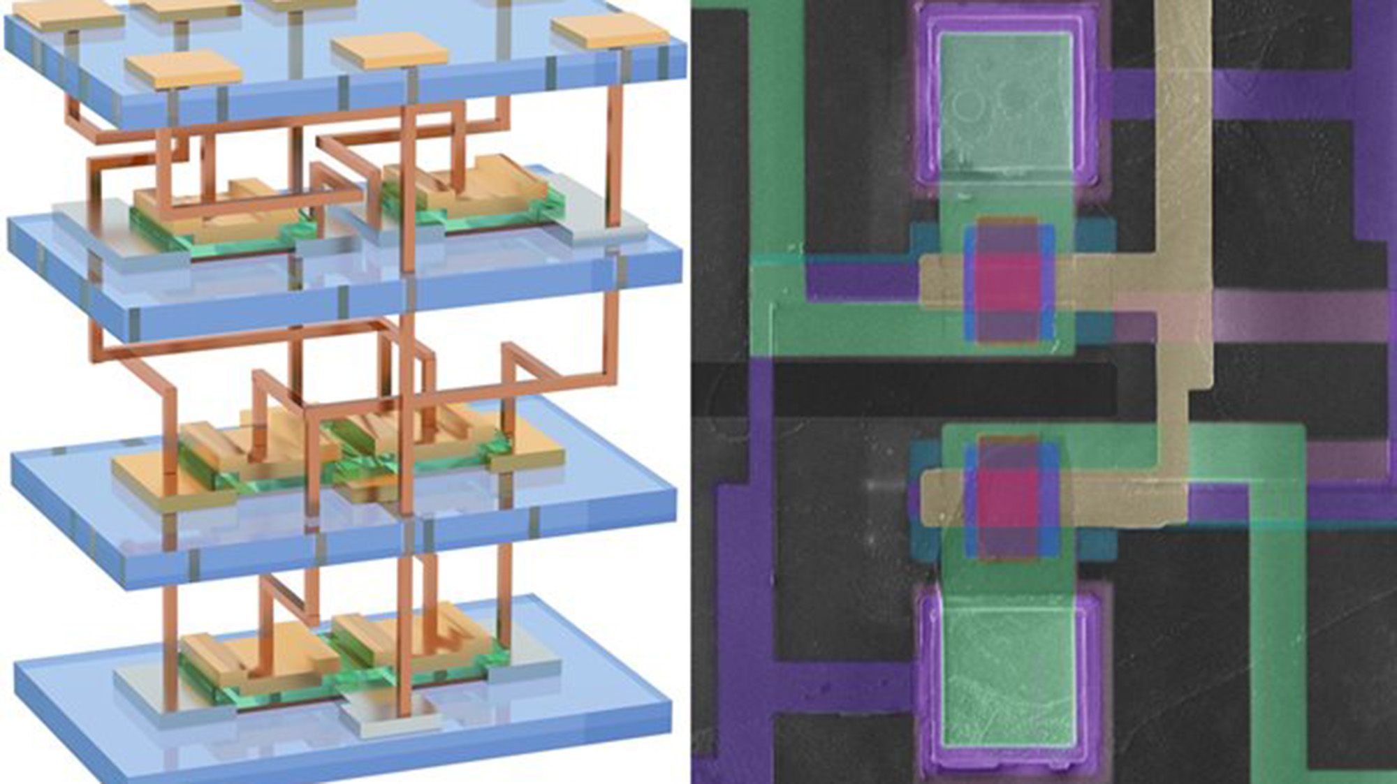
The soaring demand for artificial intelligence (AI) applications has surpassed the limitations of current semiconductor technology. However, researchers have introduced an innovative three-dimensional silicon chip that aims to tackle this challenge.
In a groundbreaking study published on May 27 in the journal Nature, scientists have unveiled a method to enhance computing power by vertically stacking silicon circuits. This strategy allows for multiple layers of silicon to be engineered without compromising performance.
Vertical stacking, commonly referred to as 3D integration, demonstrates superior efficiency compared to traditional 2D chips, where silicon circuitry is spread over a flat surface. This innovative stacking technique minimizes the distance data must travel and reduces the power needed for data transmission.
The new 3D chip employs ultrathin silicon films along with low-temperature manufacturing processes to overcome hurdles encountered in existing chip architectures.
“Our method is not only low-cost and easy to implement, but it also offers several advantages over traditional methods of stacking silicon wafers,” said Blue Cao,” the lead author of the study and a professor of materials science and engineering at the University of Illinois at Urbana-Champaign noted in a statement.
Extending Moore’s Law
Since the 1960s, the miniaturization of transistors has been essential for electronics to manage more demanding applications. However, as Cao pointed out, the principle of Moore’s Law—the expectation that the number of transistors will double approximately every two years—is becoming increasingly difficult to achieve.
“When you examine the actual size of transistors, they are not decreasing, particularly regarding the pitch of the contacted gate,” Cao emphasized. The pitch refers to the width of one transistor’s gate plus the separation required from the next gate.
Get the world’s most fascinating discoveries delivered straight to your inbox.
“This restriction results from the unique material properties of silicon and fundamental principles of quantum mechanics. To sustain the trend of increasing microprocessor performance, we must consider strategies beyond merely packing more devices onto a single layer.”
Researchers believe that vertical integration across multiple layers is crucial for engineers to adhere to Moore’s Law, enabling a more significant number of transistors on the chip.
“At present, storing a single bit of information necessitates six microelectronic devices called transistors on a single plane,” stated Cao, drawing an analogy to crowded cities where expanding vertically is often the solution. “This approach offers the same functionality while minimizing spatial footprint and improving data communication between layers.”
Scientist Gordon Moore analyzed a graph illustrating Moore’s Law.
Addressing Heat Challenges
While stacking isn’t a new concept, vertical integration (building layers directly atop one another) can lead to thermally dense configurations. Researchers indicate that the production of high-quality silicon chips demands temperatures reaching 1,832°F (1,000°C).
However, once the first chip layer is established, such extreme temperatures can damage the metal interconnects needed for further layers. Consequently, the “thermal budget” for additional layers—the maximum heat tolerance before deterioration—drops to 752°F (400°C), as noted by Cao. This can lead to issues with both performance and reliability.
Manufacturers have attempted to mitigate this challenge by utilizing monocrystalline silicon alternatives for top layers in 3D stacked silicon chips. Unfortunately, these materials, including amorphous and nanocrystalline metal oxides, carbon nanotubes, and polycrystalline silicon, can pose their own performance and reliability challenges, as highlighted in the study.
To navigate this obstacle, Cao and his team embraced a method termed “monolithic integration.” This innovative technique entails manufacturing all chip components on a single substrate rather than separately assembling them later.
To create each chip, the researchers developed an ultrathin silicon nanofilm and employed a roll laminator to transfer it onto a substrate containing the foundational layer.
Using this method, the maximum temperature needed for a strong bond is merely 392°F (200°C)—one-fifth of the conventional heat requirement. Moreover, the transferred film measures close to 10 nanometers in thickness, comparable to that of proteins, in stark contrast to conventional wafers that typically range from 500 to 700 micrometers (500,000 to 700,000 nanometers). Their thinness provides mechanical flexibility and allows them to conform to the underlying surface, as Cao elaborated.
The outcome is a three-layer 3D chip containing 625 transistors each. While this is minimal compared to billions of transistors now possible in existing chips, the researchers maintain that their technology presents significant power efficiency advantages. It’s demonstrated that the current flowing through their chip is at least three to four times stronger than that in monolithic chips created from alternative materials.
The pivotal question remains whether these innovative 3D silicon chips can transition from experimental setups to commercial applications. This study underscores the potential of a chip comprising three stacked layers, with scientists indicating that future developments may involve adding even more layers.
Bao Lam, Yong Man Yu, Hyunjun Nam, Su Chi Nee, Shomik Chatterjee, Shalu Rakeja, Jiang Ming Zuo, and Qin Kao. Monolithic three-dimensional integration of silicon transistors. Nature 2026. Doi: 10.1038/s41586-026-10496-6
Your knowledge about ancient devices might surprise you! Test your skills with our engaging Calculation quiz!
Source: www.livescience.com