


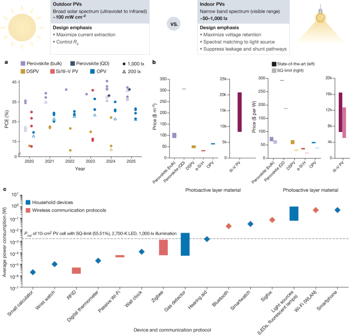
Research cited in the source material shows how indoor photovoltaics and energy-harvesting technologies are being developed to power low-energy Internet of Things (IoT) devices, wireless sensors and other electronics. The work spans organic, perovskite, silicon, III–V, dye-sensitized and hybrid solar cells, as well as wireless power transfer, device reliability, scalable manufacturing and environmental compliance. A recurring challenge is that indoor lighting is far weaker and spectrally different from sunlight, requiring materials, interfaces and testing methods designed specifically for low-light conditions.
Indoor photovoltaics for connected devices
The IoT’s expansion into laboratories, buildings and cities has increased interest in sensors that can operate without frequent battery replacement. Earlier work examined IoT experimentation in the laboratory and smart-city environments, while later studies explored large-area electronics powered wirelessly and batteryless Bluetooth Low Energy devices operating from ambient light.
- Perkel, J. M. “The Internet of Things comes to the lab.” Nature 542, 125–126 (2017). Article PubMed
- Portilla, L. et al. “Wirelessly powered large-area electronics for the Internet of Things.” Nature Electronics 6, 10–17 (2023). Article
- Sanchez, L. et al. “SmartSantander: IoT experimentation over a smart city testbed.” Computer Networks 61, 217–238 (2014). Article
- Sultania, A. K. & Famaey, J. “Batteryless Bluetooth low energy prototype with energy-aware bidirectional communication powered by ambient light.” IEEE Sensors Journal 22, 6685–6697 (2022). Article
- Chen, J. H., Chen, Y. S. & Jiang, Y. L. “Energy-efficient scheduling for multiple latency-sensitive Bluetooth low energy nodes.” IEEE Sensors Journal 18, 849–859 (2018). Article
- Raza, U., Kulkarni, P. & Sooriyabandara, M. “Low power wide area networks: an overview.” IEEE Communications Surveys & Tutorials 19, 855–873 (2017). Article
Why indoor light requires different solar cells
Indoor photovoltaic devices operate under illumination levels and spectra that differ substantially from outdoor sunlight. Research has therefore focused on selecting absorber materials with suitable bandgaps, reducing energy losses and matching devices to sources such as LEDs and other artificial lights. Indoor photovoltaic studies have covered organic materials, wide-bandgap perovskites, silicon, III–V compounds and dye-sensitized cells.
Reviews and experimental studies have examined indoor photovoltaic markets, energy harvesting from ambient light and heat, the performance of photovoltaic cells under low irradiance, and the mechanisms that limit conversion efficiency in indoor conditions.
- Mathews, I., Kantareddy, S. N., Buonassisi, T. & Peters, I. M. “Technology and market perspective for indoor photovoltaic cells.” Joule 3, 1415–1426 (2019). Article
- Yan, B. et al. “Indoor photovoltaics awaken the world’s first solar cells.” Science Advances 8, eadc9923 (2022). Article PubMed PubMed Central
- Tan, Y. K. & Panda, S. K. “Energy harvesting from hybrid indoor ambient light and thermal energy sources for enhanced performance of wireless sensor nodes.” IEEE Transactions on Industrial Electronics 58, 4424–4435 (2011). Article
- Nasiri, A., Zabalawi, S. A. & Mandic, G. “Indoor power harvesting using photovoltaic cells for low-power applications.” IEEE Transactions on Industrial Electronics 56, 4502–4509 (2009). Article
- Hamadani, B. H. “Understanding photovoltaic energy losses under indoor lighting conditions.” Applied Physics Letters 117, 043904 (2020). Article
- Juang, S. S. Y. et al. “Energy harvesting under dim-light condition with dye-sensitized and perovskite solar cells.” Frontiers in Chemistry 7, 209 (2019). Article PubMed PubMed Central
Organic and perovskite approaches
Organic photovoltaic research has targeted wide-bandgap and non-fullerene acceptors, lower energetic disorder, improved interfaces and flexible devices. The cited studies report indoor organic photovoltaic efficiencies of 30%, 30.6%, 31% and more than 33% under specified artificial-light conditions, while other work has investigated one-micrometre-thick harvesters, long-term stability and wireless power transfer.
Perovskite research has focused on wide-bandgap compositions, ion–dipole interactions, grain-boundary stress, interface dipoles, triple-cation formulations and bandgap engineering. The references also address reliability, lead-free alternatives, degradation mechanisms and the manufacture of large-area modules.
Organic photovoltaics
- Cui, Y. et al. “Wide-gap non-fullerene acceptor enabling high-performance organic photovoltaic cells for indoor applications.” Nature Energy 4, 768–775 (2019). Article
- Wang, W. X. et al. “High-performance organic photovoltaic cells under indoor lighting enabled by suppressing energetic disorders.” Joule 7, 1067–1079 (2023). Article
- Wang, T. et al. “One-micron-thick organic indoor light harvesters with low photocurrent loss and fill factors over 67%.” Journal of Materials Chemistry A 9, 13515–13521 (2021). Article
- Kim, S. H. et al. “Fine-tuning of the inner sidechain of donor polymers for efficient indoor organic photovoltaics.” Journal of Materials Chemistry A 11, 12130–12139 (2023). Article
- Luo, S. W. et al. “Optimizing spectral and morphological match of nonfullerene acceptors toward efficient indoor organic photovoltaics with enhanced light source adaptability.” Nano Energy 98, 107281 (2022). Article
- Bi, P. et al. “Achieving 31% efficiency in organic photovoltaic cells under indoor light using a low energetic disorder polymer donor.” Journal of Materials Chemistry A 11, 983–991 (2023). Article
- Wang, W. et al. “Indoor organic photovoltaic module with 30.6 % efficiency for efficient wireless power transfer.” Nano Energy 128, 109893 (2024). Article
- Kim, T. H. et al. “High-efficiency (over 33 %) indoor organic photovoltaics with band-aligned and defect-suppressed interlayers.” Applied Surface Science 610, 155558 (2023). Article
- Zhang, T. et al. “A medium-bandgap nonfullerene acceptor enabling organic photovoltaic cells with 30% efficiency under indoor artificial light.” Advanced Materials 34, 2207009 (2022). Article
- Kim, T. H. et al. “Record indoor performance of organic photovoltaics with long-term stability enabled by self-assembled monolayer-based interface management.” Nano Energy 112, 108429 (2023). Article
- Lu, X. et al. “Increase in the efficiency and stability of large-area flexible organic photovoltaic modules via improved electrical contact.” Nature Energy 9, 793–802 (2024). Article
- Lee, M. J. et al. “Tailoring hole-selective contacts via self-assembled monolayers for advancing indoor organic photovoltaic and capacitor devices.” Chemical Engineering Journal 481, 148481 (2024). Article
- Saeed, M. A. et al. “Bidentate mode coordinated Ti3CNTx MXene-controlled interfacial engineering enables high-performance indoor organic photovoltaic devices.” Chemical Engineering Journal 495, 153404 (2024). Article
- Dayneko, S. V., Pahlevani, M. & Welch, G. C. “Indoor photovoltaics: photoactive material selection, greener ink formulations, and slot-die coated active layers.” ACS Applied Materials & Interfaces 11, 46017–46025 (2019). Article
Perovskite photovoltaics
- Wang, K. L. et al. “Ion–dipole interaction enabling highly efficient CsPbI3 perovskite indoor photovoltaics.” Advanced Materials 35, 2210106 (2023). Article
- Chen, C. H. et al. “Full-dimensional grain boundary stress release for flexible perovskite indoor photovoltaics.” Advanced Materials 34, 2200320 (2022). Article
- Jagadamma, L. K. & Wang, S. Y. “Wide-bandgap halide perovskites for indoor photovoltaics.” Frontiers in Chemistry 9, 632021 (2021). Article PubMed PubMed Central
- Jiang, S. et al. “Efficient perovskite indoor photovoltaics with open-circuit voltage of 1.15 V via collaborative optimization of CsPbI2Br layer and hole transport layer.” Small Methods 6, 2200624 (2022). Article
- Heo, J. et al. “High open-circuit voltage wide-bandgap perovskite solar cell with interface dipole layer.” Small 20, 2404784 (2024). Article PubMed PubMed Central
- Jošt, M., Ajdič, Z. & Topič, M. “Performance of triple-cation perovskite solar cells under different indoor operating conditions.” ACS Applied Materials & Interfaces 16, 62195–62202 (2024). Article PubMed PubMed Central
- Albishi, M. S. et al. “Bandgap engineering for efficient perovskite solar cells under multiple color temperature indoor lighting.” Materials Advances 7, 4160–4170 (2026). Article
- Chen, C. H. et al. “Reliable perovskite indoor photovoltaics for self-powered devices.” National Science Review 12, nwaf242 (2025). Article PubMed PubMed Central
- Kundu, S. & Kelly, T. L. “In situ studies of the degradation mechanisms of perovskite solar cells.” EcoMat 2, e12025 (2020). Article
- Abdel-Shakour, M., Wang, J. F., Wang, H. & Meng, X. Y. “Lead-free perovskites for indoor photovoltaics.” Applied Physics Letters 127, 163312 (2025). Article
Silicon, III–V and dye-sensitized devices
Other approaches remain important where transparency, stability, high voltage or specialized manufacturing are priorities. The cited literature includes transparent thin-film silicon cells with reported conversion efficiencies of 36% without photodegradation, hydrogenated amorphous silicon carbide, III–V cells and GaInP absorbers. It also covers dye-sensitized solar cells, including devices reported to exceed 30% indoor efficiency and tandem cells reported above 25%.
- Kao, M. H. et al. “Low-temperature growth of hydrogenated amorphous silicon carbide solar cell by inductively coupled plasma deposition toward high conversion efficiency in indoor lighting.” Scientific Reports 7, 12706 (2017). Article PubMed Central
- Kim, G. et al. “Transparent thin-film silicon solar cells for indoor light harvesting with conversion efficiencies of 36% without photodegradation.” ACS Applied Materials & Interfaces 12, 27122–27130 (2020). Article PubMed
- Klitzke, M. et al. “Optimization of GaInP absorber design for indoor photovoltaic conversion efficiency above 40%.” Applied Physics Letters 127, 023301 (2025). Article
- Li, J. et al. “A brief review of high efficiency III-V solar cells for space application.” Frontiers in Physics 8, 631925 (2021). Article
- Mokkapati, S. & Jagadish, C. “III-V compound SC for optoelectronic devices.” Materials Today 12, 22–32 (2009). Article
- Haridas, R. et al. “Indoor light-harvesting dye-sensitized solar cells surpassing 30% efficiency without co-sensitizers.” Materials Advances 2, 7773–7787 (2021). Article
- Elmorsy, M. R. et al. “High-efficiency tandem DSSCs based on tailored naphthalene sensitizers for indoor DSSC efficiency above 25%.” Scientific Reports 15, 44135 (2025). Article
- Tian, H. N. et al. “Efficient organic-dye-sensitized solar cells based on an iodine-free electrolyte.” Angewandte Chemie International Edition 49, 7328–7331 (2010). Article
- Ibrayeva, A. et al. “Enhancing the stability and efficiency of dye-sensitized solar cells with MIL-125 metal-organic framework as an electrolyte additive.” Scientific Reports 15, 5883 (2025). Article
From laboratory cells to practical modules
Moving from small cells to deployable systems requires reliable measurement, electrical interconnection, flexible substrates, scalable coating and stable module designs. The cited work includes methods for characterizing organic photovoltaics and other devices under artificial low irradiance, studies of variable-demand standalone PV systems, and approaches to module-level interconnection and substrate reuse.
- Hamadani, B. H. & Campanelli, M. B. “Photovoltaic characterization under artificial low irradiance conditions using reference solar cells.” IEEE Journal of Photovoltaics 10, 1119–1125 (2020). Article
- Saito, H. et al. “Performance evaluation method of organic photovoltaics under indoor light condition.” Electrochemistry 86, 363–370 (2018). Article
- Parsons, D. E., Koutsourakis, G. & Blakesley, J. C. “Performance measurements for indoor photovoltaic devices: classification of a novel light source.” APL Energy 2, 016110 (2024). Article
- Posadillo, R. & Luque, R. L. “Approaches for developing a sizing method for stand-alone PV systems with variable demand.” Renewable Energy 33, 1037–1048 (2008). Article
- Hong, S. et al. “High-efficiency large-area perovskite photovoltaic modules achieved via electrochemically assembled metal-filamentary nanoelectrodes.” Science Advances 4, eaat3604 (2018). Article PubMed Central
- Shalan, A. E. “Challenges and approaches towards upscaling the assembly of hybrid perovskite solar cells.” Materials Advances 1, 292–309 (2020). Article
- Xu, Y. B. et al. “Structural design for efficient perovskite solar modules.” Solar RRL 5, 2000733 (2021). Article
- Dai, X. et al. “Pathways to high efficiency perovskite monolithic solar modules.” PRX Energy 1, 013004 (2022). Article
- Helmers, H. et al. “Processing techniques for monolithic interconnection of solar cells at wafer level.” IEEE Transactions on Electron Devices 57, 3355–3360 (2010). Article
- Shoji, Y. et al. “Substrate reuse of hydride vapor phase epitaxy grown-GaAs solar cells for low-cost photovoltaics.” In Proceedings of the 2023 IEEE 50th Photovoltaic Specialists Conference (PVSC) (IEEE, 2023).
- Horng, R. H. et al. “Thin film solar cells fabricated using cross-shaped pattern epilayer lift-off technology for substrate recycling applications.” IEEE Transactions on Electron Devices 59, 666–672 (2012). Article
- Welser, R. E. et al. In Solar Cells – New Approaches and Reviews (ed. Kosyachenko, L. A.), 247–277 (IntechOpen, 2015).
- Mariani, P. et al. “Graphene-based interconnects for stable dye-sensitized solar modules.” ACS Applied Energy Materials 4, 98–110 (2021). Article
Reliability, materials and environmental considerations
Indoor photovoltaic deployment also depends on long-term stability, material safety and the ability to integrate devices into real environments. The cited sources include studies of light-induced degradation in amorphous silicon, perovskite degradation mechanisms, lead-free perovskites, European restrictions on hazardous substances and REACH requirements. Other work has examined practical lighting-adaptive systems for wireless sensor communication and the use of ambient hybrid solar cells.
- Staebler, D. L. & Wronski, C. R. “Reversible conductivity changes in discharge-produced amorphous Si.” Applied Physics Letters 31, 292–294 (1977). Article
- Klaver, A. & van Swaaij, R. A. C. M. M. “Modeling of light-induced degradation of amorphous silicon solar cells.” Solar Energy Materials and Solar Cells 92, 50–60 (2008). Article
- Sim, Y. H. et al. “Lighting-environment-adjustable block-type 3D indoor PV for wireless sensor communication.” Scientific Reports 13, 17846 (2023). Article PubMed Central
- Michaels, H., Benesperi, I. & Freitag, M. “Challenges and prospects of ambient hybrid solar cell applications.” Chemical Science 12, 5002–5015 (2021). Article
- European Commission. “Restriction of Hazardous Substances in Electrical and Electronic Equipment (RoHS).” (2011).
- European Commission. “REACH Regulation.” (2016).
Benchmarks and broader photovoltaic context
The source also cites efficiency charts and reports from the National Laboratory of the Rockies and Fraunhofer ISE, along with studies of conventional silicon heterojunction cells and recent advances in perovskite module processing. These references provide broader context for comparing indoor technologies with photovoltaic research conducted under other operating conditions.
- National Laboratory of the Rockies. Best Research-Cell Efficiency Chart (2026).
- Philipps, S. & Warmuth, W. Photovoltaics Report. Fraunhofer ISE (2026).
- Lin, H. et al. “Silicon heterojunction solar cells with up to 26.81% efficiency achieved by electrically optimized nanocrystalline-silicon hole contact layers.” Nature Energy 8, 789–799 (2023). Article
- Ru, X. et al. “Silicon heterojunction solar cells achieving 26.6% efficiency on commercial-size p-type silicon wafer.” Joule 8, 1092–1104 (2024). Article
- Xie, Y. et al. “Regulating perovskite crystallization kinetics at laser scribe lines for efficient and stable perovskite modules.” Nature Communications 17, 2977 (2026). Article
- Liu, Y. et al. “Stabilized perovskite ink for scalable coating enables high-efficiency perovskite modules.” Science Advances 12, eaec0915 (2026). Article
- Georgiou, O., Mimis, K., Halls, D., Thompson, W. H. & Gibbins, D. “How many Wi-Fi APs does it take to light a lightbulb?” IEEE Access 4, 3732–3746 (2016). Article
Together, these studies describe indoor photovoltaics as an interdisciplinary field linking semiconductor materials, device physics, manufacturing, power management, wireless communications and environmental regulation. The cited research indicates that successful deployment depends not only on peak conversion efficiency, but also on spectral matching, low-light measurement, durability, module integration and the energy requirements of the connected device.
Source: www.nature.com