


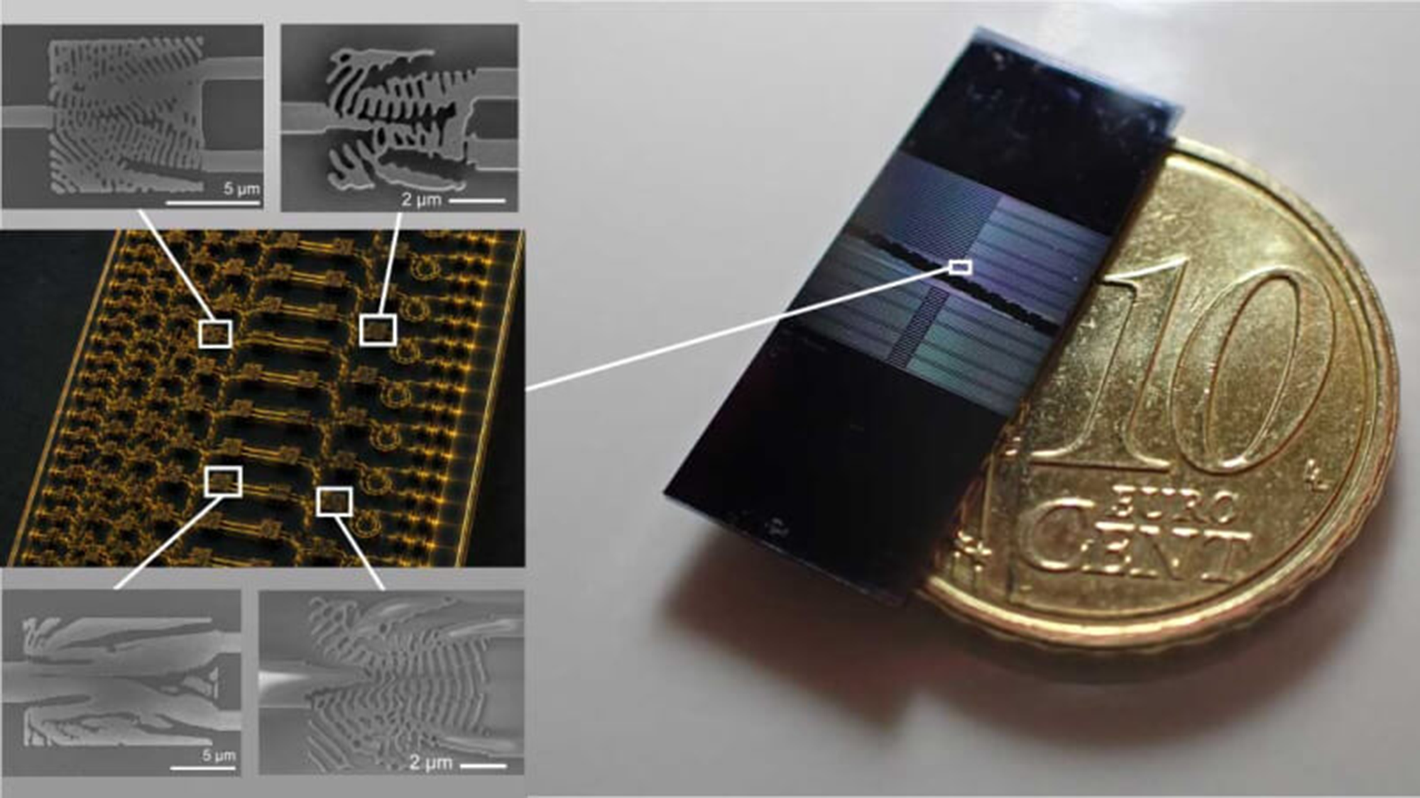
This photonic microchip is approximately the size of a penny. The enlarged view highlights AI-designed nanostructures, wavelength splitters, spatial mode sorters and mirrors integrated into a compact optical circuit.
Image credit: Tony Bi / MPL
AI-Designed Photonic Chips Could Make High-Speed Computing Far More Compact
Scientists have used an artificial intelligence algorithm to shrink three essential components of a photonic microchip by as much as 500 times. The advance creates valuable space for additional functions and could help engineers build smaller, faster and more efficient optical computing systems.
Unlike conventional electronic chips, which use electrons to process and transmit information, photonic chips use particles of light called photons. Because photons travel at the speed of light, photonic technology can support extremely fast data transfer, higher bandwidth and lower heat loss.
These advantages have made photonic chips increasingly important for fiber-optic communications, data centers, artificial intelligence, lidar systems for autonomous vehicles and quantum computing.
Rather than using metal wires, photonic integrated circuits direct light through micrometer-scale channels called waveguides. Other components, including wavelength splitters, spatial mode sorters and optical mirrors, separate and control different light signals within a space far narrower than a human hair.
Latest videos from
Live Science
The researchers used AI-generated designs to manufacture all three components at an exceptionally small scale. Their findings were published May 28 in the journal Nature Communications.
The additional space created by these miniature components could allow engineers to add more optical functions to a single chip. The study also shows that AI can create practical nanophotonic structures that would be extremely difficult to design manually.
How AI Creates Tiny Photonic Components
The researchers first specified how each component should manipulate light. They also gave the AI system manufacturing limits, including restrictions on how sharply the nanostructures could bend.
The algorithm then worked backward from the desired optical performance. It generated, tested and refined numerous designs until it found nanostructures capable of producing the required results while remaining suitable for fabrication.
“With inverse design, we can define what we want the light to do, and through optimization we find structures that make it happen — often in ways humans cannot draw,” said study lead author Toby Bi of the Max Planck Institute for the Science of Light, according to a research statement.
The same design framework produced three different optical functions: directing light according to its wavelength, sorting light by spatial mode and reflecting light to form a compact optical cavity on the chip.

The AI system repeatedly optimized the shape of each component for use in an integrated photonic circuit.
Image credit: Aditya Paul
Photonic components are traditionally designed by hand. Engineers typically begin with an established geometry and gradually adjust it to meet new performance requirements. Although reliable, this process is slow and limits the number of possible designs that can be explored.
Silicon Nitride Helps Reduce Optical Loss
To improve performance, the team built the components from relatively thick silicon nitride. The material was approximately 400 to 800 nanometers thick, compared with roughly 150 to 400 nanometers for conventional silicon structures.
The thicker silicon nitride helped confine light more effectively and reduced unwanted optical losses. The resulting mirror measured about 11 micrometers long and reflected up to 98.5% of incoming light while suppressing unwanted spatial patterns.
When two mirrors were positioned on opposite sides of a waveguide, light reflected between them more than 100 times before escaping. This result demonstrated the low-loss performance of the silicon nitride platform.
The wavelength splitter measured approximately 5 micrometers across — about the size of a single bacterium — while the spatial mode sorter was slightly larger.
AI-Designed Photonic Chips Move Toward Practical Applications
The researchers have demonstrated the three compact components individually, but the next challenge is combining them into a complete photonic integrated circuit. A successful integration would enable fully functional optical chips with far greater component density.
“These results demonstrate the feasibility of customized photonic components that are compact and resistant to manufacturing errors, paving the way for scalable and high-performance integration in silicon nitride-based photonic systems,” the researchers wrote in their study.
AI is already being explored throughout the semiconductor design and manufacturing process. In some cases, machine-learning tools have reduced chip-design timelines from weeks to hours while helping lower production costs.
Other AI systems can generate effective semiconductor layouts from relatively brief instructions. Google’s AlphaChip, for example, uses machine learning to plan chip layouts, including designs used in the company’s mass-produced artificial intelligence processors.
Bi, T., Zhang, S., Bostan, E., Liu, D., Paul, A., Ohletz, O., Harder, I., Zhang, Y., Ghosh, A., Alabbadi, A., Kheiri, M., Zeng, T., Lu, J., Yang, K., and Del’Haye, P. (2026). Reverse engineered silicon nitride nanophotonics. Nature Communications, 17(1).
Source: www.livescience.com